With graphics cards ranging from budget-focused models to power-hungry beasts, choosing the right GPU for your needs can feel daunting. While raw power and benchmarks matter, deciphering spec sheets is equally important for informed purchasing decisions.
This guide aims to simplify the process by defining key technical specifications found across modern gaming graphics cards. From architecture and clock speeds to memory interfaces and cooling designs, understanding each term enables apt comparison between offerings. Whether looking at budget-level or high-end choices, grasping these essentials allows one to discern the optimal feature set and value.
With new generations arriving yearly from AMD and Nvidia, specifications evolve constantly. Therefore, consumers must learn the language. This becomes especially relevant when considering long-term potential or specific workloads. Creative professionals, for instance, have different priorities over casual players.
By breaking down often confusing jargon, this special report makes the selection process less ambiguous. Readers will gain insights into the core technologies and how they impact real-world functionality. Armed with this knowledge, anyone can confidently choose the best graphics card tailored to their budgets and needs. So let us start our tour by examining the basic building blocks of modern GPUs.
Architecture
At the core of every graphics card lies its architecture - the foundation that dictates its capabilities. The architecture encompasses the underlying design and manufacturing process used to build the GPU.
The last decade saw monumental leaps with each generation. Nvidia introduced Fermi, Kepler, and Maxwell and later made giant strides with Pascal and Turing. Meanwhile, AMD offered GCN, followed by Polaris, Vega, and RDNA. These leaps brought orders of magnitude more processing power and game-changing technologies.

The latest architectures from both vendors showcase their future-proofing endeavors. Nvidia’s Ada Lovelace doubles down on RTX while AMD’s RDNA3 introduces Infinity Cache and rearranged compute units for greater efficiency.
The architecture essentially acts as the framework on which other specs are built. Its sophistication influences aspects like raw horsepower, memory bandwidth, and power efficiency. Manufacturers also optimize architectures over multiple iterations to enhance performance per watt.
For buyers, properly comprehending a GPU’s architecture provides invaluable context regarding its capabilities and potential longevity against future titles. It reveals the foundation of ray tracing, resolution scaling, and more.
NVIDIA’s Ada Lovelace vs AMD’s RDNA3
Nvidia’s latest Ada Lovelace architecture builds upon the success of Ampere with enhanced ray tracing and AI acceleration. Its multi-chip module design with advanced TSMC 4N process unlocks unprecedented levels of performance.
Meanwhile, AMD’s RDNA3 architecture significantly strides with its 5nm manufacturing. The addition of a 3D V-Cache stacked over the die significantly boosts bandwidth. Optimized compute units and hardware-accelerated ray tracing bring it on par with Nvidia.
Both architectures deliver giant performance-per-watt gains over previous generations. Ada Lovelace leverages techniques like multi-instance GPU and optimized cache hierarchies. RDNA3’s rearchitected schedulers help maximize efficiency across workloads.
Gamers and creators can leverage Ada’s RTX capabilities like DLSS 3.0’s large frame generation boost. RDNA3 debuts Infinity Cache and Radeon RSR for crisp image quality.
The competition between these power-efficient architectures raises the bar for PC graphics. While Nvidia retains performance leadership, AMD has closed the gap with an enormously scalable design of its own at competitive price points. This bodes well for continued advancement.
CUDA Cores / Stream Processors
At the heart of modern GPU computing are the basic processing units known as CUDA cores on NVIDIA cards and stream processors on AMD cards. These thousands of small cores are dedicated to performing highly parallelizable tasks. More CUDA/stream cores allow for more computations and higher flop counts.
The latest NVIDIA Ada Lovelace chips can have over 16,000 CUDA cores, while AMD’s top RDNA3 models pack upwards of 6,000 stream processors. These core counts contribute greatly to advantages like real-time ray tracing and AI-driven effects that demand massive parallelism.

More cores also translate directly to higher raw graphics and computing performance. Games and other workloads are divided into many threads that can then be worked on simultaneously across the cores. This is what facilitates rendering cutting-edge titles at high resolutions and frame rates.
Interestingly, cores on the same GPU are not all identical. Modern architectures include different types optimized for specific tasks like integer/floating point and ray tracing work. This specialization allows work to be distributed more efficiently.
For buyers, paying attention to a GPU’s CUDA/stream processor count during comparisons can indicate its general horsepower and suitability for workload demands. More cores will typically age stronger over multiple years of use.
Tensor Cores and RT Cores
Beyond traditional compute units, modern GPUs include dedicated hardware to accelerate specific cutting-edge workloads. NVIDIA GPUs contain Tensor Cores optimized for neural networks and deep learning. Meanwhile, Tensor and RT Cores together handle ray tracing tasks.
Tensor Cores debuted on the Volta architecture and have since evolved. The latest Ada Lovelace GPUs pack up to 512 Tensor Cores, delivering a spectacular level of processing power for AI tasks. This feeds applications of deep learning supercomputing.

For real-time rendering, RT Cores engage in path tracing by intersecting rays with scene geometry. NVIDIA’s RT Cores have advanced through multiple iterations, with Ada Lovelace versions 4x faster than Ampere. AMD also introduced ray accelerators with RDNA2 and enhanced them in RDNA3.
The specialized cores work in conjunction with regular CUDA/stream processors. While the latter handle traditional graphics work, Tensor and RT Cores take charge of their specific functions. This partitioning avoids bottlenecks and maximizes efficiency.
For users, the presence of dedicated accelerated cores ensures leading-edge computational capabilities beyond raw horsepower alone. Their performance impacts professional AI work as well as next-gen gaming features like ray tracing.
Graphics Card Memory
The memory subsystem is a crucial aspect impacting a GPU’s overall performance. Its capabilities are determined by factors like the bus width, memory technology, bandwidth, and video RAM capacity.
Manufacturers try advancing all these specs across generations and even within the same families. For example, NVIDIA’s RTX 4090 boasts a 512-bit interface with 21Gbps GDDR6X modules, giving over 1TB/s bandwidth. AMD’s RX 7900 XTX reaches around 1 TB/s as well when it comes to memory bandwidth.

Complex games pushing textures, effects, and high-res assets require greater memory heft and quick access. Understanding these specs allows matching a GPU appropriate for workloads and resolutions while future-proofing for years.
Bus Width
Bus Width refers to the pathway connecting the graphics processor to the VRAM chips. Wider buses allow more data to transfer simultaneously. High-end current GPUs utilize 384-bit and 512-bit memory interfaces for massive throughput.
Memory Technology
VRAM Technology indicates whether it uses GDDR6, GDDR6X, or upcoming memory types. GDDR6X pushes bandwidth boundaries and first appeared on the RTX 3090. Newer cards may adopt upcoming technologies like GDDR7.
Memory Bandwidth
Memory Bandwidth is the maximum data rate the VRAM can provide to GPU every second, measured in Terabytes per second. Higher bandwidth allows faster access to texture and render data. Top cards push over 1 TB/s to keep cores well-fed.
VRAM Size
VRAM Size denotes the total onboard video memory available. More VRAM allows larger textures and more complex game worlds/scenes without sacrificing quality. Today’s most powerful GPUs include 12GB or more.
Memory Clock
Memory Clock describes the frequency at which VRAM modules cycle data. Clock speed is a contributing factor to effective bandwidth. Memory overclocking aims to push this higher.
Effective Memory Clock
Effective Memory Clock is the VRAM data transfer rate, determined by multiplying the memory clock by a number based on memory technology such as GDDR6X. Higher effective clocks boost bandwidth.
Texture Mapping Units and Texel Rate
TMU counts have steadily risen with each generation. Early 2000s cards had as few as 4 TMUs, versus today’s high-end models flaunting 500+ TMUs. More TMUs allow more textures to be sampled and blended simultaneously, reducing load times.
The effective use of these units ties to another metric - the Texel Rate. Measured in Gigatexels per second, it refers to the number of texture pixels a GPU can process in a single second utilizing all TMUs together.
A higher Texel Rate indicates greater abilities to apply detailed textures efficiently across many triangles on-screen. It affects how “busy” graphics appear and supports larger, more immersive environments.
For context, Nvidia’s RTX 4080 manages a Texel Rate of 761.5 GTexel/s. The RTX 4090 reaches a colossal 1,290 GTexel/s thanks to 512 TMUs churning at over 2 GHz of core clock. AMD is similarly pushing boundaries - the RX 7900 XTX hits 959.6 GTexel/s
Newer titles demand more realistic materials and finer textures influencing everything from vegetation to character clothing. A sufficiently high Texel Rate ensures such richness loads quickly without hang-ups. It directly feeds perceived image quality.
TMU and Texel specifications showcase a GPU’s texturing muscle for complex dynamic scenes. Professionals in CAD, video, and 3D work also leverage the metrics for texture-heavy rendering tasks. Over time, higher counts retain capabilities against advancing texture resolutions in use.
Paying heed to these overlooked but important specs enable wiser purchasing informed of potential capabilities for textures - a core graphics concern for eye-catching visual fidelity. Combining them with other metrics builds a rounded assessment.
Render Output Units and Pixel Rate
Graphics processing requires not just raw compute power, but specialized units dedicated to rasterization and pixel rendering. Raster Operator (ROP) units handle the final pixel coloring and writing to the display.
Modern GPUs house dozens of ROP partitions to process pixels rapidly in parallel. For example, the RTX 4090 contains 192 ROPs spread across its multiprocessor cores. More ROPs allow higher pixel fill rates for smooth, intricate graphics.
Pixel Rate refers to the number of pixels a GPU’s ROPs can process in a second. Measured in Gigapixels per second (GPixel/s), it impacts frame rendering times and supports resolutions/refresh rates directly.

NVIDIA’s upcoming RTX 4090 boasts an incredible 443.5 G Pixel/s pixel rate thanks to its 176 ROPs churning at over 2GHz. This handily outpaces prior gens and enables silky gameplay even at 4K.
Likewise, AMD’s top RX 7900 XTX card reaches 479.8 GPixel/s. Both companies continue optimizing ROP designs across tiers to balance pixel throughput.
Higher pixel rates benefit gamers and creative work. For gaming, it helps sustain high resolutions even under intense effects and explosions on screen. Creatives see quicker viewport refreshes while modeling or video editing at high resolutions.
Interestingly, the pixel rate alone does not dictate maximum display outputs. Additional factors like memory bandwidth and driver optimizations influence supported refresh rates in the real world.
Still, the pixel rate gives a clear indicator of raw pixel-pushing capabilities to handle future advances in fidelity and resolution standards. Evaluating ROP counts alongside this spec offers strong clues about a GPU’s pixel processing muscle.
With displays and content rapidly improving, today’s ROP and pixel rates future-proof hardware for several years against increasingly demanding creative pipelines and AAA game visual experiences.
Base Core Clock and Boost Core Clock
At the heart of any GPU’s performance metrics are its core clock speeds - namely the base clock and boost clock. These dictate the speed at which the graphics processor and its constituent components operate.
The base clock is the default clock speed, usually, the minimum guaranteed by manufacturers under normal usage. For example, NVIDIA’s RTX 4080 has a base clock of 2.2GHz.
However, thanks to powerful cooling and on-die voltage regulators, GPUs are capable of surpassing base speeds dynamically using a technique called boosting. The boost clock states the maximum increased clock achievable briefly under certain conditions. The RTX 4080 can boost up to 2.5GHz and even higher during gaming.
This boosting behavior is managed automatically in real time based on variables like thermal headroom and power consumption. It allows clock spikes for enhanced performance during intensive scenes before naturally downclocking to stabilize temps.

Higher base and boost clocks translate directly into increased processing throughput, directly impacting framerates, resolution capabilities, and heavier effects workloads. Even a 200-300MHz boost can make a tangible difference.
Of course, other specifications like shader/texture/ROP units also determine maximum theoretical throughput. But in simple terms, a GPU with a higher boost clock will almost always outperform the same GPU with lower clocks at the same workload.
Proper cooling solutions are indispensable to sustaining boost frequencies consistently rather than having extensive thermal throttling. Overclocking then pushes speeds even further assuming cooling can handle the increased heat output.
Understanding core clock facilities judging a GPU’s processing grunt and how it might hold up over several intensive games or apps. The right cooling ensures advertised boosts are reliably delivered.
Display Outputs
To transmit graphics from the GPU to your display, cards include diverse ports matching various connection types. The assortment of display outputs opens options for setup flexibility.
Modern high-end GPUs utilize a combination of HDMI and DP ports supporting resolutions up to 8K at 60Hz. The DisplayPort connects with higher bandwidth for massive resolutions at 120-240Hz over a single cable.
Newer cards may adopt DisplayPort 2.0 allowing even greater single-cable outputs. The RTX 4090 features three DP2.0 ports enabling 8K165 or 4K240Hz output.

Creative workhorses leverage multi-monitor sprawling workflows, aided by outputs like Dual-Link DVI for high refresh rates on older displays. Some cards preserve legacy ports but these are disappearing in favor of versatility through miniDisplayPort and USB Type-C alternatives.
The selection of ports lets you choose between common TV connections through HDMI versus cutting-edge G-Sync/FreeSync monitors on DisplayPort. Cross-manufacturer compatibility removes hassles in upgrading components at different times.
Understanding a GPU’s display interfaces helps ensure it aligns with your existing display configurations for seamless plug-and-play functionality and supports desired resolutions whether gaming or productivity.
PCI Express Interface
For a GPU to communicate with the rest of the system, it requires an interface to the motherboard. All modern consumer graphics cards utilize the PCI Express (PCIe) bus standard.
The PCIe version and lane count determine the maximum bandwidth between the GPU and other components. Higher-end cards today employ PCIe Gen5 with 16 lanes, providing vastly more throughput than older PCIe 3.0 cards.
This bandwidth facilitates pushing immense resolutions and rapid multi-GPU rendering. The latest cards fully saturate Gen5 speeds with over 16GB/s bidirectional transfers.

Lane counts also impact bandwidth - where Gen4 saw primarily x16 connections, some mainstream GPUs now utilize x8 to save costs. However, x16 remains standard for flagship cards to avoid bottlenecks.
Understanding a GPU’s PCIe specs reveals how freely it can communicate, whether ray tracing, AI workloads or bandwidth-hungry VR may face restrictions. It also hints at longevity against future standards - PCIe Gen5 maintains compatibility for years.
For assembling a system, confirming your motherboard supports the card’s PCIe interface avoids performance limitations from hardware bottlenecks outside the GPU itself.
Power Consumption and Power Connectors
One of the most important specifications for a GPU is its power rating - the maximum wattage it draws under load. This is usually denoted by the Thermal Design Power (TDP).
TDP reflects how much heat a card can generate and what cooling solutions are required. Higher-power models today exceed 350W TDP while mid-range sit around 200W. This impacts things like power supply needs and case thermal design.
To safely provide such demanding wattages, modern high-end graphics cards employ 6-pin, 8-pin, or even 6+2-pin PCIe power connectors directly from the PSU. The RTX 4090 uses a massive new 16-pin connector capable of 600W delivery.
These specialized power connectors bypass the weak 75W provided through the PCIe slot alone. Their placement near the GPU die keeps length and resistance low for stability.

A card’s power configuration hints at how vigorously it can boost clocks under sustained loads. Dual 8-pin RTX cards can typically overclock farther than single 8-pin models for this reason.
While an 850W PSU can run 350W cards today, its headroom permits 500W+ models further down without replacement.
Efficient power regulation on the die helps offset demands, advancing performance per watt. Still, adequate juice through the right connectors fosters stability at demanding resolutions.
Manufacturers strive to reduce connector counts over time too. Comparing models based on TDP ratings and included power plugs helps compatibility planning with existing modular PSUs and case real estate. Overall system requirements are critical.
Understanding graphics cards' appetite maintains efficient, durable systems aligned with your power and thermal overhead to maximize the lifespan of components.
Cache Size
To help improve performance and memory efficiency, GPUs employ hierarchical caches similar to CPU designs. Caches store recently or frequently accessed data to allow quicker retrieval than from slower memory.
The size and type of cache contribute greatly to a GPU’s effective bandwidth and throughput. Modern high-end models integrate large L1 and L2 caches.
For example, NVIDIA’s RTX 4090 houses 72 MB of L2 cache and 16 MB of ultra-fast L1 cache. This massively expands on prior generations and facilitates smoother rendering by reducing memory latencies.
Bigger caches also aid workload transitions like when streaming in new textures. They help optimize memory compression for greater effective bandwidth.
Cache specifications reveal how “smart” the memory architecture is at anticipating future access patterns. This intelligently hides latency variations from slow DRAM. A larger cache correlates to stronger performance consistency across a wide variety of games and applications.
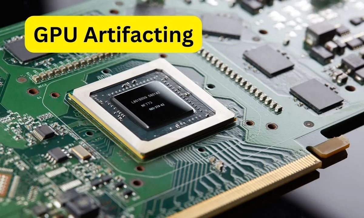
Graphics Processor Specifications
Modern GPUs are highly complex chips defined by a variety of design and manufacturing traits. These manufacturing specs depict the immense capability squeezed into ever-tinier footprints. Understanding them highlights the profound technological progress driving gaming to astonishing levels almost inconceivable just a few short years ago. Let’s examine these core specs across recent examples.

GPU Name and Variant
GPU Name and Variant distinguishes models - like NVIDIA’s GeForce RTX 4090 versus the RTX 4080 16GB. Variants often differ just in memory or core counts.
Foundry
Foundry refers to the chip manufacturer, usually Taiwan Semiconductor Manufacturing Co (TSMC) or Samsung Foundry for bleeding-edge nodes. TSMC produces the latest Lovelace and RDNA3 designs on superior 5nm processes.
Process Size
Process Size indicates the minimum component detail possible - currently, 5 nm allows over 20 billion more transistors in the same die area as 7nm. Smaller nodes deliver huge performance/watt benefits.
Transistor Count
Transistors are the basic on/off electronic switches packed into the silicon die. Peak GPUs now exceed 76 billion, doubling every couple of generations thanks to process advances. Denser designs facilitate added functionality.
Transistor Density
Density measures transistors per square mm - the RTX 4090 packs over 125 million, enabling enormous parallelism. Higher density maximizes capabilities within physical size constraints.
Die Size
Die Size discloses the raw area of silicon, typically 300-600+ square mm. Larger yields more components but comes at a manufacturing cost premium. Chips now tip 600mm^2 demonstrating the complexity required for leading graphics.
Board Design Specifications
While the silicon chip lies at the heart of any GPU, manufacturers design full circuit boards housing additional onboard components. These influence compatibility, thermals, overclocking headroom, and more.
Overall, board specifications are instrumental in compatibility planning. Custom water blocks may alter dimensions. Understanding stock specs avoids assembly mishaps in cramped enclosures unfit for thermally aggressive designs.
Slot Width
Slot Width defines the space occupied in the PC case. Most mainstream adhere to the standard dual-slot at 2 slots tall (approx. 4cm), though multi-slot coolers exist. Custom boards may exceed this.
GPU Length
Length measures the PCB extension past the PCIe slot, typically 25-30cm maximum to prevent interference. Longer designs facilitate beefier coolers/VRM but reduce case compatibility.
GPU Width
Width indicates card thickness. Higher-end models approach 3 slots (~6cm) using voluminous cooling apparatus like 3.5 slot designs that span multiple bays. Wider boards demand open-case layouts.
GPU Height
Height refers to the card’s rise above the motherboard. Coolers adding extra centimeters necessitate taller case clearance to prevent damage during installation.
Board Number
Board Number refers to PCB revisions by manufacturers. Updates may integrate improved components, layouts, or BIOS versions over generations. Board partners also customize proprietary designs.
Voltage Regulator Module
Digital voltage regulation circuitry, capacitors, chokes, and PWM controllers populate the GPU board to ensure clean, plentiful power. Higher-quality components aid stability under overclocks.
Graphics Features
Beyond core metrics, GPUs are defined by supported industry standards enabling rich functionality. These graphics APIs dictate capabilities.
Verifying a GPU aligns with your software ensures harnessing the intended functionality. Creative plugins, games, versions, and workstation tasks have varying requirements that must be met for productivity.
Graphics standards evolve rapidly. While older APIs retain compatibility, the latest spec compliance future-proof upgrades against advancing needs beyond traditional gaming like raytracing, AI upscaling, or simulation software.

DirectX
DirectX governs Windows games/apps. The Newest cards support DirectX 12 Ultimate for DXRaytracing, variable rate shading, and other cutting-edge effects. Prior chips may top at DX11, restricting newer titles.
OpenGL
OpenGL is the cross-platform 3D graphics standard for operating systems beyond Windows. Current GPUs adhere to at least the flexible OpenGL 4.6 specification.
OpenCL
OpenCL allows parallel computation on GPUs for non-graphics work like 3D modeling, physics simulations, or cryptocurrency mining. Support enables tapping graphics processors for general-purpose tasks.
CUDA
NVIDIA CUDA provides programming tools to fully wield enormous GPU parallelism for compute-intensive workloads like AI inferencing, scientific research, or deep learning. Availability unlocks vast accelerator abilities.
Shader Model
Shader Model reflects DirectX shader capability - SM 6.6 enables extreme tessellation/geometry for lush next-gen title terrains and objects. Earlier cards plateau below SM 6.0 limiting cutting-edge effects.
Vulkan
The Vulkan API delivers low-overhead graphics across Windows, Linux, and more for high performance. Support equips flexible solutions for VR/AR applications demanding blistering framerates.
Theoretical Performance
GPU calculations are performed using different data precisions and formats dependent on the numeric type required. Understanding supported formats is important for applications.
Lower precisions like FP16 boost speed by processing more data concurrently within VRAM and cache limitations. Higher precisions like FP64 slow down throughput but suit precision-critical tasks.
Selecting a GPU that matches your software’s numeric precision requirements optimizes workload performance versus fallback routines to different data types that underutilize the hardware. It ensures full acceleration of tasks.
FP16 Performance
FP16 or ‘half precision’ uses 16-bit floating point values for maximum throughput. This is optimal for tasks like AI inference needing reduced precision over FP32. All recent GPUs heavily feature FP16 compute abilities.
FP32 Performance
FP32 or ‘single precision’ utilizes the common 32-bit floating point. It provides more precision than FP16 for graphics, physics simulations, and most game computations while still enabling considerable parallelism. This is universal on consumer cards.
FP64 Performance
However, pure FP64 or ‘double precision’ at 64 bits is far more compute-intensive. As such, only specialized workstation GPUs aim for parity between FP32 and FP64 performance. Gaming chips feature limited or no native FP64 hardware.
GPU Overclocking
While manufacturer specifications define reference hardware baselines, tweaking settings allows pushing chips even farther through overclocking. Done properly, this can significantly boost performance - sometimes nearly matching the next SKU up.
Done cautiously, overclocking maximizes a GPU’s potential lifespan before needing hardware upgrades, especially when overclocks maintain lower temperatures than boost algorithms. Undervolting complements this for low-effort speed boosts. But precautions against damage are prudent for the most aggressive tweaking.

Overclocking
Overclocking increases the core and memory clock speeds above stock speeds. This is done through software like MSI Afterburner or NVIDIA/AMD control panels. Higher clocks yield more processing power if stability can be maintained through cooling and voltage adjustments.
Underclocking
Conversely, underclocking intentionally runs components below stock speeds - rarely done unless reducing power/noise for workstation tasks. Undervolting also down-volt chips for lower temps, noise, and power draw at stock clocks.
Auto-Overclocking
Generally, modern GPU Boost handles aggressive auto-overclocking well out of the box. However, manual overvolts prod additional headroom by incrementally raising voltage/power limits within safety thresholds. Liquid nitrogen cooling pushes the limits of silicon.
Memory Timings
Over-tightening memory timings can also net free performance. But pushing too fast often corrupts frames rather than artifacts requiring a restart to recover. Peripheral overclocks to GDDR6X memory and VRAM controllers yield gains without core instability issues.
Undervolting
Undervolting aims to reduce thermal/power consumption footprints without sacrificing performance. Precision tweaking saves watts and extends boost durations. Thermal and power throttling impacts are reduced, boosting regular workloads.
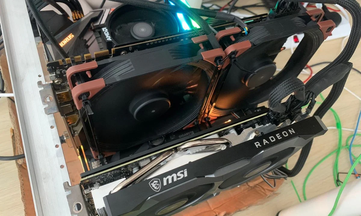
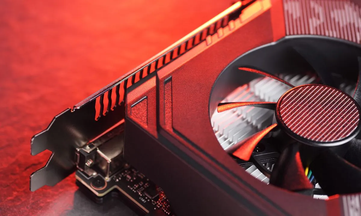
GPU Design Features
Dissipating escalating chip densities and power demands necessitates innovative thermal designs. Coolers vary drastically between models.
Between cooling solutions, proper ventilation sustains factory boost frequencies consistently through intensive workloads vital for harnessing a card’s full abilities. Understanding these thermal design specifications avoids potential temperature issues from inadequate ventilation.

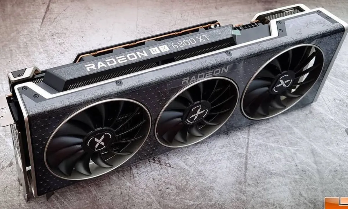
Tri-fan Design
High-end cards may utilize 3+ fan designs like NVIDIA RTX 4090 variants. Triple axial fans provide enormous airflow. A precise fan curve controls abate noise versus two fans.
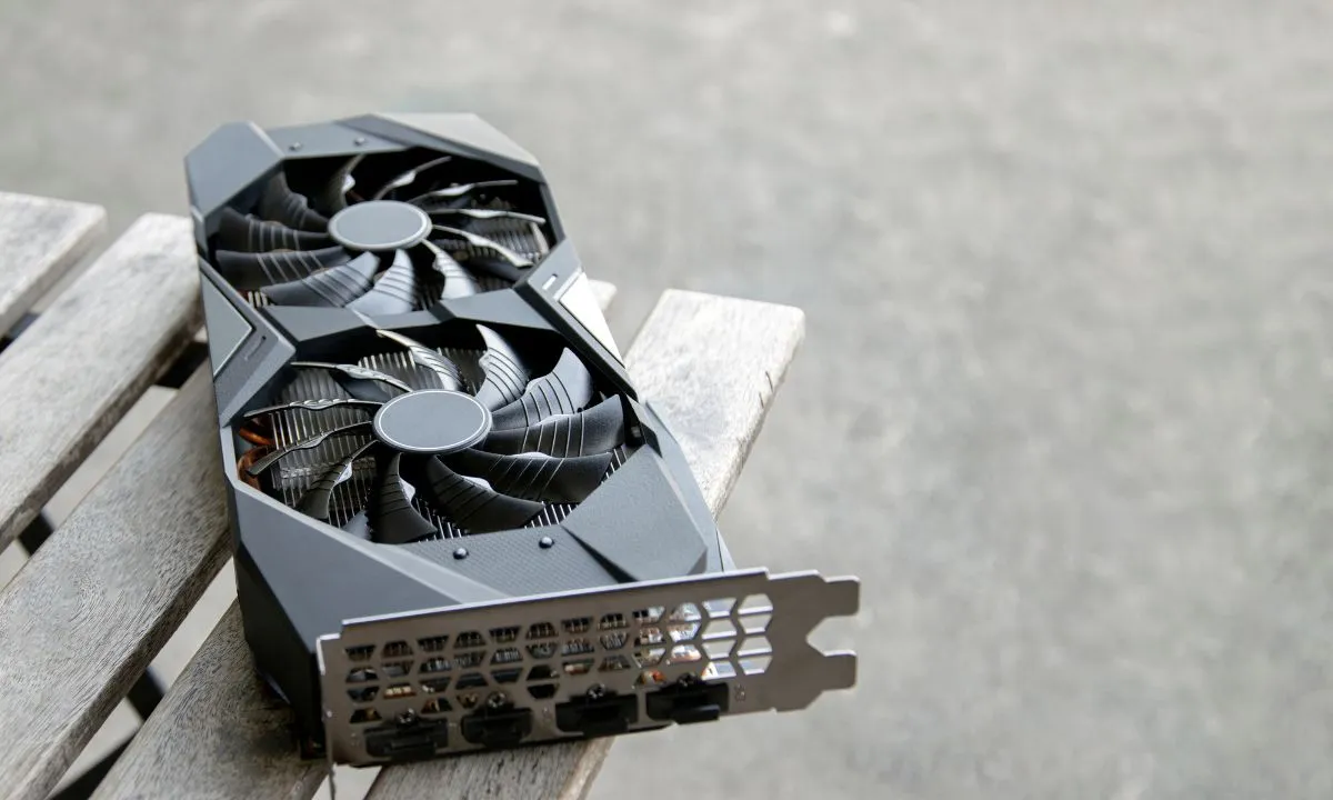
Dual-fan Design
Dual fan coolers balance enhanced cooling with additional weight and thickness versus single fan blower options. Dual-axial designs efficiently cool the GPU, VRAM, and VRM with targeted chambers.
Single-fan Design
Some mainstream GPU models utilize a single axial fan cooler. This more compact solution draws air directly onto the heatsink fins rather than exhausting laterally. While less robust than dual-fan designs, single fans remain a cost-effective option for mid-range gaming when case airflow is sufficient to expel hot air efficiently.
Blower Style Design
Single blower style cards historically vented outward rather than exhaust inside cases. However, modern blowers combine intake and lateral exhaust for optimal interior ventilation without excess heat buildup.
Heatsink Design
Heatsink design also evolves - vapor chamber models encircle the GPU die and components. Microchannels efficiently transfer heat away into heatpipes which funnel hot air over large aluminum fin stacks before exhaust.
Some designs utilize open-die direct contact between heatsink surfaces and naked silicon, vastly accelerating thermal transfer. Cutting-edge pads and pastes improve conductivity.
GPU Backplate
Many high-end cards integrate rigid reinforced GPU backplates behind the PCB. These increase rigidity for heavy coolers while reflecting heat conducting through the board back toward the heatsink, improving longevity.
Air Dynamics
Sophisticated airflow optimizations inside dense cooling shrouds manipulate thermal dynamics for accelerated dispersal compared to reference designs. Adequate ventilation through dedicated chassis intakes and exhausts are crucial.
GPU Variants
While GPU manufacturers produce reference boards, partners create customized variants tailored for specific uses. Variants boast factory overclocks and upgraded cooling/digital designs.
Understanding the intended target audiences of each unique variant aids in pairing the optimal solution with specific needs or aesthetics to fully leverage a board’s finer qualities over reference PCBs. Premium models especially maximize investment potential.
Board partners like MSI, Asus, Gigabyte, Sapphire, XFX, Zotac, PowerColor, and others infuse personality through naming.

Popular NVIDIA Variants
MSI Gaming X Trio variants leverage robust triple fan coolers and OC profiles for silent yet potent gaming. Precise Twin Frozr designs emphasize acoustic finesse.
ASUS ROG Strix models establish prestige gaming fortitude. Lengthy PCBs and stylish LED lighting combine with innovations like DirectCU coolers.
Gigabyte AORUS variants flaunt fully custom PCBs, premium components, and Windforce RGB cooling optimized for masterful experiences.
Zotac provides budget-focused lines like the Twin Edge but is renowned for extremes with the Amp Extreme featuring impressive factory overclocks and robust triple fan cooling.
Popular AMD Variants
ASUS TUF Gaming cards balance longevity and dependability for resilience.
MSI GAMING X emphasizes robust aesthetics and performance.
XFX Speedster trim boards excel at stock speeds with Mercury cooling.
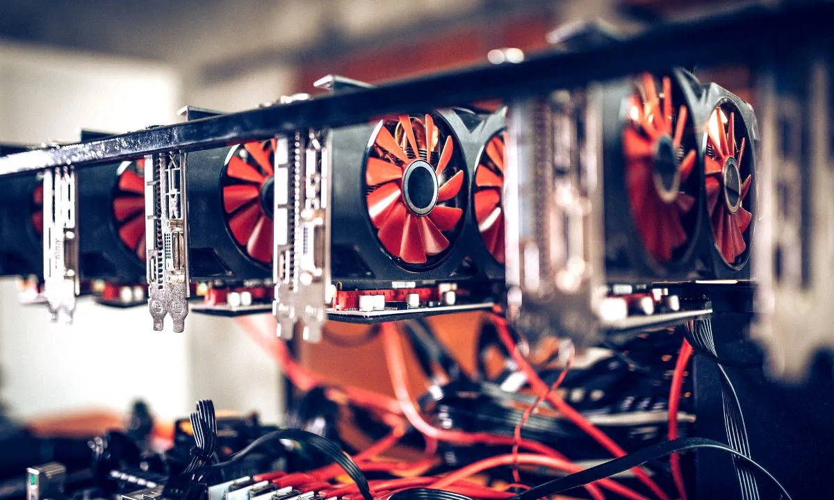
PowerColor variants overcommit to overclocking headroom and mining potential.
Sapphire is a top AMD board partner known for reliable and well-cooled Nitro+ and Pulse variants well-suited for gaming and mining.
Custom Designs
Custom designs can bring higher factory and overclocking ceilings along with embellishments. Diverse ventilation, PWM fan curves, capacitor selections, and PCB layouts augment reference thermal/power delivery.
Liquid Cooling / Hybrid Cooling
Variants also launch with factory liquid cooling or hybrid air/liquid configurations from companies like EVGA Hydro Copper or Asus ROG Strix LC.
GPU Drivers
Ensuring a GPU has the latest stable drivers is crucial for peak performance, features, optimizations, and stability. Drivers interface hardware with operating systems and applications.

NVIDIA Drivers
NVIDIA releases GeForce drivers quarterly with Game Ready versions for major titles. These optimize performance/experience. Studio drivers prioritize creators. Alternate drivers like NVIDIA CUDA support GPU computing.
NVIDIA GeForce Experience
Alongside drivers, NVIDIA provides GeForce Experience. This desktop application automatically detects hardware, updates drivers, optimizes settings, suggests optimal preferences, and records gameplay footage. ShadowPlay likewise enables seamless streaming/recording.
AMD Drivers
AMD releases Radeon Adrenalin quarterly with Game Optimization and Studio drivers. They provide the same functions as NVIDIA but for Radeon GPUs and compatibility with FreeSync technology.
AMD Radeon Software
AMD utilizes Radeon Software for driver management and optional Radeon Auto Overclocking for one-click performance boosts. Radeon Anti-Lag optimizes rendering for competitive gaming and ReLive enables recording/streaming.
AMD VS NVIDIA Driver Comparison
Both aim to optimize games post-launch alongside ensuring stable platform compatibility with OS/driver updates. Apps suggest optimal in-game settings or simply handle this automatically. Game filters can sharpen or enhance visuals.
NVIDIA offers additional productivity features alongside GeForce Experience like Ansel VR photography within supported titles. WhisperMode undervolts for quieter systems. The control panel remains similar to navigate than Radeon’s application.
AMD counterbalances via a more full-featured installer for advanced tweaks, options to force downclock states, and Radeon Image Sharpening for enhanced clarity. Their control panel sports a cleaner interface than older versions.
Overall both chipmakers aim to simplify the gaming experience while empowering advanced users. Timely driver releases optimize compatibility; their apps balance usability with powerful optimization and recording tools for gamers and creators. Choosing relies on software priorities and GPU brand support.
Conclusion
Graphics cards have come a long way since their inception, pushing the boundaries of real-time rendering capabilities. What was once specialized hardware for niche 3D applications is now an essential component of modern PCs, enabling immersive gaming experiences and creative workflows. As analytics of GPU specifications reveal, continuous innovation across architectures, manufacturing processes, and software brings us ever closer to photorealism.
Both AMD and NVIDIA have demonstrated relentless dedication to advancement through their respective RDNA and Ada Lovelace architectures. These lay powerful foundations for the next era of PC graphics. Features like ray tracing, variable rate shading, and AI upscaling are gradually transforming applications beyond our wildest imaginings just a few years ago. Judging by the exponentially growing transistor counts and introduction of technologies such as 3D stacking of cache, there appears to be no signs of slowing down. Creators and gamers alike can expect continually sharpening immersion.
Of course, grasping specifications remains indispensable for matching hardware appropriately to software needs. Workstation tasks demand strict adherence to standards like double precision support. Gamers benefit from comprehending factors impacting frame rates like memory bandwidth. Cryptocurrency miners leverage understanding of hash rates. With optimization an endless pursuit, specifications offer windows into technologies enabling the optimization endeavors of both manufacturers and third parties.
Looking ahead, initiatives like real-time ray tracing and advanced AI upscaling promise to obliterate long-standing uncanny valley effects. Hardware-software collaboration will generate photorealism surpassing our senses. Yet specifications also reveal ongoing struggles with thermals and power consumption necessitating innovation. Balancing strides in performance with efficiency remains paramount for sustainability.
Overall, graphics have elevated experiences beyond what was redeemable as recently as the prior generation. With the resolute improvement of specifications established over decades of competition, the graphics revolution marches ever onward toward photoreal virtual worlds accessible to all.
Judging by continual optimizations across all metrics, we can expect rendering to progress indefinitely, propelled by an innate drive to depict and interact with reality through ever more immersive lenses. Specifications serve as signposts charting this continuous march of progress.